You are using an out of date browser. It may not display this or other websites correctly.
You should upgrade or use an alternative browser.
You should upgrade or use an alternative browser.
1000w smps based on LUDO3232
- Thread starter Silvio
- Start date
behrad
Member
thanks.im fine
my hdd destroyed in last year and i lost all of files about electronic circuit
i made 2*apex sr-150 and 1*subwoofer ampli and s/c protect for ampli and vu meter and sub-filter circuit and etc... but i dont have power supply so i back and decided build this smps for my 2.1 channel ampli project
my hdd destroyed in last year and i lost all of files about electronic circuit
i made 2*apex sr-150 and 1*subwoofer ampli and s/c protect for ampli and vu meter and sub-filter circuit and etc... but i dont have power supply so i back and decided build this smps for my 2.1 channel ampli project
behrad
Member
mr silvio
u have 2 transformer winding instruction!
http://www.diysmps.com/forums/showt...ased-on-LUDO3232&p=14542&viewfull=1#post14542
http://www.diysmps.com/forums/showt...ased-on-LUDO3232&p=14756&viewfull=1#post14756
which one is correct(or better)?
i need 50-0-50 volt so i think first instruction is better for me
Silvio
Well-known member
Hello Behrad, the instruction for you will be different due to the output voltage needed is 50-0-50
Winding turns for you are primary 18 turns and secondary 6-0-6 turns. (volts per turn = 8.6v)
with these turns you will get around 52v peak on the output at around 230vac input.
Winding instruction for ETD49 N87 core
The primary and secondary should be made with 2 bundles of 4 wires each twisted together (8 wires total divided in 2 bundles) copper wire diameter is 0.5mm and frequency of operation is 65Khz
Put heat shrink tubing at the ends of the wire bundles when coming out with the wire from the bobbin.
1) Wind 9 turns of primary winding (2 bundles together)leave the rest out this should cover one layer leaving 3 mm margin at the ends of the bobbin. leave the rest of the wire out so that you wind the second part of the primary after the secondary.
2) Put 3 layers of mylar or capton tape to insulate.
3) Prepare 2 bundles of 4 wires each and wind half the secondary starting from the center tap and finish on the pins of the bobbin at one end.
Note put the winding in the center of the bobbin and fill the gap on the sides with a piece of tape cut to size to fill the gap between winding and the bobbin cheek so that you have enough to come level with the winding.
4) wind the second part of the secondary starting also from the center tap as in instruction 3. fill also the sides to get an even surface for the last part of the primary. Put 3 layers of tape to insulate.
5) Take the remaining wire left from the first half primary and wind the last half of the primary(9turns) and finish at the pins. insulate with 3 layers of tape.
Lastly you can wind the auxiliary windings as needed and calculate at 8.6v per turn ( example for 15-0-15 volts you need 3 turns bifilar (25v) then regulate with 7815 and 7915 for the preamplifier voltage. for 12 for fan motor supply you need 2 turns (17v) and regulate at 12v.
I suggest you take a look at this video so that you understand more of what am I saying in the instructions.
https://www.youtube.com/watch?v=_K3ixhcTYFg&t=5s
good luck. Silvio
First Time DIY on SMPS 600W
Hi Everybody
First time i have doing my DIY on SMPS. I followed attached schematic. Time of testing PWM board alone it is fine and waves are very good. After connecting to main PCB( Now i am using general purpose board) first time it burnt IR2110 and SG3525. IRFP400 also shut. Second time there is a big explosion and again IR2110,Sg3525 and IRFP400 also shut. I am totally disappointed with this result. Please guide me.
Thanks & Regards
Samarendra DasView attachment 600W SMPS V2.4.pdf
Silvio
Well-known member
Hello mituadas, I am sorry for what happened. The circuit has been built by a lot of diyers and it works. I am sure you have something wired wrong. I also see that you do not use a series lamp with the mains as a current limiter. You must use a 100w lamp so that if something is not right it will save the circuit. I also see that you have a lot of wires running around and it is not good especially from the drive circuit board to the mosfets. Long runs may pick up stray signals and will arrive distorted to the gates of the fets. You must mount the fets and heatsink on the testboard together with the drive circuit. The paths here should be short as possible.
Please check the following
1) See that the high side drive is going to the high side fet and not the other way round. See also that the half bridge wiring between the mosfets is correct according to the schematic.
2) Check the wave forms arriving at the fets by only switching on the auxiliary supply. Some SG3525 bought from China have a deformed wave form when driven more than 12vdc. (put a few series diodes with the aux line to bring down to 12v and check waveforms with an oscilloscope.)
3) Are you sure the transformer has no shorted turns in the winding. Try a transformer from an old computer smps
I did not see it in any of the pictures you sent me.
4) For the time being use smaller value capacitance on the bulk side like 330uf x 200v instead of 1200uf. The energy stored in these capacitors is large and if something is wrong they will still blow your circuit even if you have a current limiter (100w lamp). Use small capacitance (1000uf) on the secondary output until you get smps working.
5) Did you check the soft start circuit alone? Does it has a 2 second delay before the relay latches?
6) Did you check the protect circuit alone and see that it works?
7) Change the dead time resistor from 100 ohms to around 150 ohms for the time being so that you will be sure that the mosfets are not switching on together.
8) Make sure that the mosfets have good insulation between them and are properly isolated. I do not see any mica insulators under the mosfets.
9) Put a 4.7K resistor between gate and source of each mosfet to prevent false triggering
Lastly be careful in what you do mains voltage is deadly if you get electrocuted. You are doing this at your own risk.
Last edited:
Many many thanks to you Mr Silvio. I will follow all the guide lines given by you. My SMPS is in basic stage. I do not have Main PCB also. I am testing this using general purpose PCB board. I have made transformer as per your guide lines from a reputed Transformer manufacturer. I am suspecting your Point no 7 may be the culprit. How to check both signals(HI/LO) at a time? I have tested only LO side wave forms. Today I will prepare new PWM board and let you know.
Thanks
Thanks
Silvio
Well-known member
One issue I identified that as per schematic SG 14 pin connected to IR 12 and 11 to 10. But my PWM PCB which i made is SG 14 to IR 10 and 11 to 12. Will it make any difference??
It is important that the low side switch on first, this will charge up the bootstrap capacitor. Be careful and check the datasheets of the sg3525 and also of the IR 2110. Low out of SG must go to low in of the IR. Also for the High side Hi out of sg with high in of IR.
Check the wave form out of the IR 2110 This is what the gates are getting. Hook up a couple of 1K resistors from the output of the IR. one from low out to ground and the other from high out to VS if i remember correctly. You will power up only the auxiliary and not the mains. They should be both working. You can check the wave form there on both channels.
Silvio
Well-known member
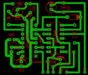
The circuit board wiring is good. The only thing I notice is that you should put the decoupling capacitors (100nf) closer to the supply pins of the ICs as possible . This will shunt out any stray inductance and any noise trying to enter the chips. You could widen the space between the ICs to gain more space for the 100nf cap especially to the SG supply input. Another solution is to solder it directly on the copper side of the board.
Last edited:
Silvio
Well-known member
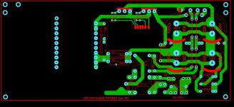
Today I am able to complete primary side of Main SMPS PCB. I got one Sprint Layout from Internet and modifying as per my requirment
View attachment 6924
Take care of the spacing between the traces. For the mains input you must have at least 3mm between line and neutral. On the 420 volt rail the spacing should be 4mm.
The trace width for a one once copper board is 1mm per amp. Calculate what amperage you have on all the rails and adjust as necessary.
Spacing between primary and secondary circuits is a minimum of 5mm.
Regards Silvio.
Silvio
Well-known member
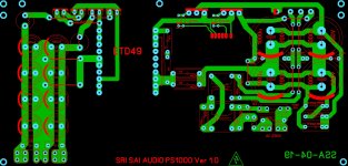
Layout and spacing is good but the trace width is not enough. The traces should be according to the current handling of the smps. You can calculate at 1mm per amp. For example for the mains input you will be having around 5 to 6 amps so the traces should be 5 or 6mm. The half bridge traces that is from the mosfets to the transformer are going to carry around 8 amps so these should be around 8mm or so. The output rails to the diodes and after the diodes will depend on the output voltage. For instance if you have 50-0-50 on the output then to make up for 1000 watts of power the width of the traces should be around 10mm ( 1000W / 100v = 10amps)and the ground trace should be the same width or more. The latter should be made to your convenience. Traces carrying high current should be kept as short as possible.
Good luck.
Silvio.
Silvio
Well-known member
I see a mistake in your setup. The fuse is shorting the mains input through the soft start resistors. You also did not include the shorting relay to short out the input softstart resistors. You will need a delay timer for the relay (2 or 3 seconds). The relay is needed to minimize losses. For an amplifier you will usually need an output for the preamp circuit (15v-0-15v) You will also need an output to drive the cooling fan motors 12v or 24v. Maybe also a 5v for a blu tooth etc. These can all be included in the smps.
Good luck.
Silvio.
Last edited:
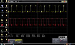
Today while I am testing my PWM module i have observed the following, which is not looks good.
1. SG module both the waves are good.
2. From IR2110 LO side i am getting good wave form as well as 4.6v. But from HI side i am getting 9.XX v and VS(Pin 5) getting 9.xx v.
My power supply is 12.1v(From PC SMPS)
Last time also i burnt my PWM board and IRFP 460 mosfet.
Please guide me where is the mistake.
Thanks
Silvio
Well-known member
Today while I am testing my PWM module i have observed the following, which is not looks good.
1. SG module both the waves are good.
2. From IR2110 LO side i am getting good wave form as well as 4.6v. But from HI side i am getting 9.XX v and VS(Pin 5) getting 9.xx v.
My power supply is 12.1v(From PC SMPS)
Last time also i burnt my PWM board and IRFP 460 mosfet.
Please guide me where is the mistake.
Thanks
As far as I can see is that you should get 12v on the low side and a little less (11.4v) on the high side. This is because you are driving the high side with a diode. Be sure that the bootstrap diode is a fast type like FR104 or uf4003 etc. Please check that out A SG3525 is driving high side of Ir2110 and out B driving the low side.
The high side out of the IR2110 usually seems a low amplitude pulse because this is only the charge of the bootstrap capacitor. Do not worry about this because the resistance of the mosfet gate is very low and the voltage will rise.
make your voltage measurement using the scope as the multimeter will only give you the RMS voltage which is lower than the peak.
When you are satisfied with the output of the IR2110 you can connect to the smps. Put a series 100w lamp with the mains supply. This will save your mosfets in the event if something is wrong. The lamp will show you if you are correct or not. This will light up very briefly and will go off again. This is due to charging the input capacitors on start up. If it is not well the lamp will light up and limit the current going to the smps.
I hope that helps


