zeus_threat
Member
Hi Microsim thanks for the reply sim shows too much offset with 741 in single supply mode LM393 gives very good sim results am completing testing on the overtemperature circuit
")
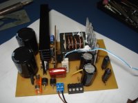
 and working on the main power pcb also
 Its almost identical to the prototype layout i need to rethink if everything is positioned properly before going further
The exposure box is being rebuilt. I've noticed how bad those fluorescent tubes can get as they heat up a dark layer starts to build up and reduces exposure surface. This shouldn't happend with the UV leds.
Hi giololucas i've looked at your design. honestly i got a voltage drop from +-35 to +-32V when loading the SMPS from light to medium-high. you are mentionning 2 problems
1) the heavy voltage drop could be something inherent with IR2153 that has quite a high deadtime built in but it coud also be someting else
2) 20V ripple is huge with my basic capacitors didn't even yield such high ripple. It didn't even bother to measure it as i could not even see it when loading the SMPS.
Personally i wouldn't put a controller board facing mosfets like that just put your scope probes in front and you will see how much EMI they radiate when they conduct the board is also likely to heat up severely with heat radiated from the mosfet + heatsink on heavy loading.
Could you show GS and DS waveforms at safe level? Make sure you take necessary precautions to isolate everything and do this at a safe voltage level <40V
My guess but am not sure is that the mosfets are radiating back energy to IR2153 OP pins causing cross conduction. In turn protection triggers and latches the OP. Your caps energy get sucked out by the load since the mosfet stopped conducting causing the heavy ripple you see and it repeats like a cycle.
Look at Ludo and Microsim 1KW SMPS they are based on IR2153 its properly laid out
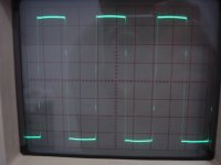
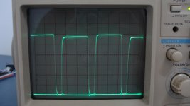
I think what you showed in previous attachment was the primary transformer wave form right? It looks basic simple but the proper functioning of any SMPS lies in those wave shapes. Another advice if you can't load both SMPS secondaries at once with 350W load both simultaneously with a smaller load. but nothing won't replace a proper OC/OV/UV/OT set of protections. Not to get your design complicated but that fuse you have used won't prevent your mosfet and ic from blowing up in case something goes wrong.Hi your waveforms look good for GS with SMPS unloaded But you will have to do more measurements GS + DS unloaded and loaded it will tell you if everything is correct. Also if possible try to measure the current flowing through the primatry loaded and unloaded it can be done with a current probe in case you have one or a current sense trasnfo and be careful to do this with gradually increasing voltage. Don't try it straight at full voltage even with isolation. The current wave form should be like a triangular waveform for the inductor and like a square wave with an upward slope for the mosfet like in this document: http://www.coremaster.com/appnotes/an108.pdf on page 2
A is the mosfet current B is the transformer voltage C is the transformer current am sure you must already know all that
Now another point its strange that all those ripple drop by x10 by just isolating the SMPS, were your scope and SMPS both grounded when you made the output voltage measurement? Ground loops maybe. As far as i know all smps measurements are made with isolation either at SMPS or using differential probes.
LC pi filters or double pi filters are there to prevent interference in and out of the circuit. you can see many designs on the net even app notes not using them but it needs to be implemented that interference will either end up in your smps or in one of your home appliance. If you are on your way to adding that filter, a varistor for added surge protection won't be something excessive in that circuit. EMI and surge are the two basic thigns you need to filter before rectifying AC mains to send to your smps
Another thing as well, most proper implementations of IR2153 use a totem pole or mosfet driver at their output, have you checked if their output current is enough to charge Cgs of the 840? In some cases i have read of these buffers protecting the IC from failing when the mosfets blow up but that needs to be verified
. Hi giololucas glad to hear you got everything working and under control. Good luck for your next prototype
.