The reason I've used TL494 is because I can play with the error amplifiers. And it's got two.
I might sound stupid, but the threshold voltage for the UC3845's current sense input is 1.1V (say 1V to simplify everything). So that means 10A through a 0.1 ohm resistor. But what if I want to limit the current to 5A through the same resistor? That would be 0.5V. How do you "lower" the threshold so it would start limiting at that value? A comparator can be used, but it 1V is too low for a supply voltage.
Apart from that, I thought about what Silvio said and I had the idea of building a single rail 50V supply and then adding another push-pull stage with a 1:1:1 transformer that outputs +50V and -50V. All the regulation made at the "primary" of this transformer will reflect at both of the secondaries, and being 1:1 makes everything easier. Of course, that means double the losses and half the power.
Those error amplifiers aren't very good and still leave you with no way to do real current-mode control. While the idea of simply using one error amp for current limiting and the other for voltage limiting sounds very simple and straight forward, in practice this doesn't really work well at all. There are tons of examples online of supplies that use the TL494 in this configuration, and while I'm sure that some of them work, the results are poor when compared to other methods of control. I've built and tried many supplies like this in my early days and they just don't work as advertised. The TL494 is best suited when used in a half-bridge topology (voltage-mode control) and using external comparators to sense the voltage/current of the output and provide a simple on/off type of feedback to the TL494 (not using the internal error amps at all). There is a reason that almost every computer PSU that uses this chip, uses it in this way, or in a way that is very similar. It's done because it's cheaper to continue to use it rather than redesign the PSU that uses better components and control schemes. Although almost all of the PSU manufacturers today have trashed this design due to the new standards for power-factor and efficiency.

And no, you don't sound stupid at all, as this is what I thought when I first encountered the UC384x chips. After much more studying I realized that isn't how this chip actually works.
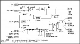
That 1.1V threshold on the ISense pin is the voltage at which the output of the chip shuts down. If you put 1.1V on the ISense pin, it doesn't matter what voltage is on the Vfb pin, the chip stops switching. This is a good way to implement a shut-down feature for a power supply.
Now, the ISense pin is actually used to sense the current flowing through the transformer's primary winding while the switches are on. Hence current-mode control. It's not for sensing the output current.
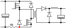
There is an internal current source (usually 1mA or 500uA) feeding the COMP pin. This, combined with the inverting error amp, keeps the COMP pin driven high when the Vfb is at 0V. As you can see in the diagram, when the COMP pin is high, there is a bit of a voltage drop across the diodes, it's divided by 3, clamped with a zener at 1V, then fed into the current comparator. Any time the voltage at ISense is higher than the voltage at the other comparator input (1V when COMP is high) it disables the output. The way you use this is as follows. You size your sense resistor, or use a current transformer, so that it gives the 1V or 1.1V to the ISense pin at whatever your transformers maximum primary current should be. This ensures that even if the secondary became shorted, the current flowing through the primary and the switching transistors could never be greater than this amount unless one of the switches failed. In the diagram below, RS is the sense resistor and the red dot is where you would take off the ISense signal. For higher power supplies with higher primary currents, a current sense transformer would be a better option to avoid the heat generated by a large power resistor. Now, as your power supply turns on and starts switching, the output voltage starts to rise. As the output voltage rises, this will cause the voltage at the Vfb pin to rise (feedback compensation circuitry is required between the output and Vfb pin.) When Vfb increases above 0V, this will cause the voltage at the COMP pin to start to fall. As the voltage at the COMP pin falls, the voltage on the current comparator also falls, which means the output of the UC384x begins to turn off at a lower current level (lower duty-cycle). Once the output hits its target voltage, the COMP pin will be close to 0V, which means that almost no current will be switched through the primary, thus providing the regulation. This current comparison happens on every cycle which gives pulse-by-pulse current limiting.
The other common, and even more simple, approach to using the UC384x chip is as follows. Pull the Vfb pin to ground level (0V), then place an opto-coupler between the COMP pin and ground. Then on the output of the supply, you can use an adjustable voltage divider style circuit to drive the opto-coupler. Once the output hits the target voltage, the opto-coupler turns on, pulls the COMP pin low, thus decreasing the duty-cycle and primary current flow. This method provides isolation between the input and output of your power supply in addition to allowing the use of external sensing circuitry. Usually a TL431 programmable shunt regulator is used to provide an easy way to switch the opto-coupler on and off.
I'm not trying to knock your ideas or anything like that, but if the goal is an adjustable lab supply with very good performance, this is a solid way to go. Even if you don't use a TSFC topology, the basic design should be an isolated SMPS tracking pre-regulator followed up by a linear regulator for each output rail. The tracking SMPS allows you to keep the input voltage to the linear regulators close to the output voltage so that heat dissipation and losses are at a minimum, and the individual linear regulators feeding each output rail allows you to have rock solid output voltages with very minimal ripple voltage. Since you brought up the idea of a TSFC in one of your early posts I was giving you solid recommendations for how to build one. Truthfully, if I were building a lab supply, I would probably build the SMPS section as a half-bridge followed by the linear regulators. Even if you built a half-bridge, there are still way better ICs than the TL494 to get the job done while still being cheap to use.
As for the idea of a fixed supply with a secondary SMPS 1:1:1 stage, you are completely right. The losses of building such a configuration would be very high when compared to other methods. This would also add much more complexity to the project while not providing any sort of benefit over the simple, straight forward designs that myself and Silvio have presented.
I've also looked at UC3845/UC3843 and SG3525 (for push-pull mode). I'm not sure if 2-switch forward can be run on duty cycle greater than 50%.

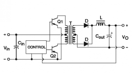
A TSFC topology can only run up to a theoretical duty-cycle of 50%. In practice, this is usually limited to 46-48% just as extra insurance to ensure that the magnetic flux within the transformer is able to completely reset to the zero point during the off-time of the switching cycle. Since a TSFC only applies current to the transformer primary in one direction, the core can saturate if the flux is not completely reset during the off-time. During the switching cycle, when the switches turn off, the flux collapses within the transformer and causes a voltage spike in the opposite polarity. The two diodes then allow the voltage across the primary to rise to just slightly above the DC bus voltage and the current from the collapsed magnetic field then flows back into the DC bulk storage caps until the current drops to zero. Since the reset voltage is only slightly higher than the DC bus voltage (1 or 2V) we can consider them equal for the calculations. Simply put, the off-time must be equal to or greater than the on-time in order to achieve proper core reset and avoid saturation. There are ways to have the transformer reset at a voltage higher than the DC bus voltage, which allows the duty-cycle to be increased above 50%, but this adds unnecessary complexity to the power supply that just isn't needed in this application.

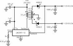
As for a push-pull topology. That is usually limited to low input voltage supplies such as those powered from the 12V in a car. Push-pull is a very poor choice when being powered from mains voltage due to the center-tapped primary. The voltage rating of the transistors/mosfets need to be more than double the DC Bus voltage to ensure they don't fail from over voltage. If the DC Bus voltage is 340V, when Q1 is on, the voltage across Q2 is double that (680V). This happens the opposite when Q2 is on, the voltage across Q1 goes to double the bus voltage. Current balance through the legs of the primary is also very important in a push-pull supply, and much more so at line level voltages. The TL494 and SG3525 have no provision to ensure that the on-time of Q1 and Q2 are both equal for each cycle. Uneven pulses can cause the flux of the transformer to become biased towards one polarity or the other during operation which can eventually lead to the core saturating and destroying the transistors. At lower voltages, such as in a car, this effect is less likely to happen the doubled voltage across the transistors becomes a non-issue.
- Brad
PS - Sorry for such a long post, but I only have time to get on here 1 day out of the week due to my job. I wish you good luck with building your power supply, and even if you don't use any of my suggestions, I hope they are at least helpful to you.

