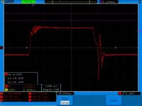
I'm going to have to agree with KX36 that your turn-off oscillations seem to be capacitance related. Your schematic with the IGBTs does seem kind of odd for a high-power 2-Switch Forward. You are correct, you should not need an RC snubber across the transformer primary. Here are some of the things I would recommend for using IGBTs in a high-power converter using this topology.
C30-C33. Your Gate-Emitter capacitors could be removed. The IRG4PC30UD is a much older GEN4 IGBT, these tend to turn-off significantly slower than they turn-on, and having this extra capacitance to drain along with the gate charge is slowing down the switching and this could be the source of your ringing at the gates. Stray inductance can cause problems as well. All of the traces and component leads between the driver IC and the Gate pin should be kept to an absolute minimum.
R23-R25. The 3R3 resistors in series with the reverse diodes on the gates. Those can be removed to further increase the turn-off speed of these devices. Your gate drivers should be capable of sinking the gate charge through the diode without this resistor.
D19 & D20. I would try removing these as well. I've never seen an RCD circuit used in this topology before. Leave the RC part there as a snubber across the switches though. 4n7 for C15 & C16 is usually the value I've ended up with for a high-power two-switch running around 50kHz. It's not a guarantee, just usually where the experimentation has led to in most cases. R29 & R30, depending on the amount of snubbing required, I've had anywhere from 50R all the way down to 4.7R to get an optimal waveform. These resistor values vary with transformer design and the type of load applied to the secondary in my experiences. Also, I've had good success with placing an RC snubber directly across the secondary of the transformer as well in cases where ringing was a problem across the secondary. It can also help some with ringing on the primary depending on the transformer design and source of the ringing.
One last thing to note; the IRG4PC30UD datasheet states that in hard-switched mode these devices are optimized for 8-40kHz. In my experience with these GEN4 I*R IGBTs, this rating is usually for bridge or half-bridge configurations and it's also usually very generous and I wouldn't recommend this U(UltraFast) device for anything over 20-25kHz. While the switching speed isn't quite as critical in a 2-Switch Forward topology, since both high and low side devices switch in phase with each other, I would still recommend going with the IRG4PC30W(WarpSpeed) device over the U/UD device if you're set on this generation of I*R devices. The turn-off delay and fall-time isn't much faster with the W version, but the turn-on delay and rise-time are about half. Also, with these IGBTs, the current carrying capability is diminished as the frequency increases, I'm assuming due to switching losses and tail current. Both the U/UD and the W(There isn't a WD) versions are 30A rated, but if you examine the graph in the datasheet for Current vs. Frequency, you'll see that at 50kHz, the UD device is only rated for about 5A while the W device is close to 9A. This could possibly make a difference in performance and full-power duty-cycle of your power supply. The W device doesn't have a built-in diode like the UD does, but in this topology they aren't always needed, and could always be added externally.
If you're really serious about building this with IGBTs. My best recommendations for switching devices would be either the HGTG30N60A4D from Fairchild. It's a fairly fast device, and you would most likely only need 2 instead of the 2x2 setup in your original schematic. This device, with a 3R gate resistor and adequate drive current, can switch a 50A, 200uH inductive load at a Vce of 390VDC at 50% duty-cycle at 50kHz.
If you don't need that much, the HGTG20N60A4D can switch a 35A, 500uH inductive load, with all other parameters the same as the 30N60. It also switches a bit faster.
But, if you need even more, the FGA30N65SMD, also a Fairchild device, has some interesting specs. It's only rated for a continuous collector current of 30A at 100*C case temperature(60A@25*C). Maximum pulsed current is 90A with the pulse length only limited by the junction temperature. This device seems as though it's more attuned for higher speed operation than what your design is using, but running this device at only 50kHz could minimize switching losses in the IGBT itself. The graph shows it's capable of switching 60A at 50kHz despite being a 30A device. This is what leads be to believe that it is intended for much higher switching frequency. The 30A@100*C switching current is clear out close to 175kHz, still pushing 20A at 300kHz.
Now I understand that the ratings given in the datasheets are probably tested in the most ideal setup that the manufacturer can come up with, and information like this when pulled from a datasheet can very much differ from real-life performance due to a multitude of factors. I will say that I have personal experience with the HGTG20N60A4D, 30N60A4D, and the 40N60A4. They are quite wonderful devices and I haven't ever been disappointed with their performance. For the TIG welder design that I'm still very slowly working on, I'm going to venture into new territory and try out Fairchild's FGH40N60SMD device. It is one of the fastest IGBT devices I've ever come across when it comes to switching large currents into an inductive load. If they turn out to be as impressive as the other Fairchild devices I've used, they will help to minimize the size of my switching stage while also minimizing the losses in that stage as well. Should work good in the PFC converter as well.
Sorry about the rambling, I hope some of this information is helpful to you. I can't really comment much on your PCB layout. I'm very much an amateur at PCB design. Sorry.


 òlll.jpg19.3 KB · Views: 67


")


