HV SMPS 12v - 500v

Virus

New member
Hi Guys.

I have been trolling the threads here on SMPS for a while, but as most SMPS are mains voltage to ±12v or so, or 12v to ±35v for car amps etc, I could not find answers relating to my questions.

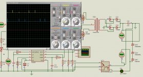
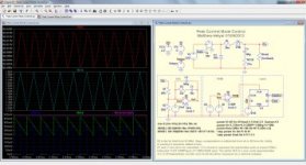
I have built SMPS's based on SG3525 and IR 2153 chip , (there is allot of information re this IC's on the web), and yes it is working,

BUT

Here is my problem:

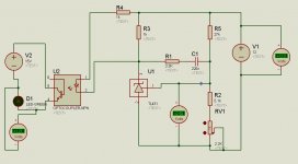
I need the earth or ground on LV side isolated from the HV side but with feedback to the chip, with normal feedback the grounds on either side are joined (unless it is free running), the only way I see this to work is by using an optocoupler, that can isolate the 2 grounds from each other and have the feedback working properly.

Therefore I humbly ask for your wisdom to be shared in this regard, if anyone has a circuit that can direct me in the right direction it would be highly appreciated. Even if I need to use use a different chip etc. it will be fine to do so.

I have a couple of question and will work at them 1 at a time, and need to get it working properly with low currant first, as this is one huge learning curves for me.

Please be patient as I have limited knowledge in electronics design etc.

Thank you Theunis
 

KX36

New member
Yes, if you require isolation between primary and secondary (as all off-line power supplies do), you need to isolate their grounds and the standard way to do this is with a primary side PWM IC and secondary side voltage error amplifier consisting of a TL431 and an optocoupler. The loop design is more complex with this topology as performance and even stability can depend on the highly variable parasitics of the opto. Type II compensation of a CMC converter is a lot easier within the limits of this topology than Type III compensation of a VMC loop.

There are alternative ways to get the analog information across the isolation boundary using special purpose ICs which might for example encode the information and/or send it through a pulse edge transformer, they would be more complex and expensive than accepting the flaws of an opto feedback loop.

www.onsemi.com/pub/Collateral/TND381-D.PDF

http://switchingpowermagazine.com/downloads/15 Designing with the TL431.pdf

http://cbasso.pagesperso-orange.fr/Downloads/Papers/The TL431 in loop control.pdf

One more thing, a little less conventional. I don't know exactly how you've arranged your 2 chip converter, but since the IR2153 is a free-running and unregulated transformer driver, it's possible use the SG3525 as a non-isolating converter (buck or boost) regulating a bus voltage on the primary side and then drive the IR2153/transformer just for the isolation. Load regulation won't be as good but at least you don't have to make big assumptions about how your opto will behave as it ages and compared to other device batches.
 

Virus

New member
KX36

Thanks for your prompt reply,

I really don't understand much of the technical and maths quoted, just need it simple for this old brain !

What would the components values be for the TL431 & opto circuit, if I am wanting a 550v secondary output on a reference voltage on a SG3525 chip?

Thanks .

Theunis
 
Last edited:

Virus

New member
TL431 Simulation

Hi KX36 and others

Attached simulation re TL431, got this diagram from the web and wanted to learn on the TL431, but the opto does not light up bright enough.

Any ideas

Theunis
 

Attachments

  • Capture1.JPG
    Capture1.JPG
    61.6 KB · Views: 119

KX36

New member
Sorry, but you can't avoid the maths on this and I can't explain it any more simply than the first link I gave. It does have worked examples for type I II and III compensation. Which of those you need depends on your plant design and control mode. Any equation with an "s" in it is (literally) complex as you're talking about how impedances change with frequency and this is to do with the -j/(2*pi*f) which you might have seen in for example RC filter formulae which you may be familiar with. You can skip over those equations at first, just be aware that an s in the numerator indicates a zero, and in the denominator a pole to give you an idea of what each part will do to the frequency response. Typically type I compensators are just a pole, type II are a zero and 2 poles and type III are 2 zeros and 3 poles and unfortunately voltage mode control often requires type III.

I don't think many people around here can help much with compensated feedback loop design as few "SMPS" here have any sort of intentional feedback or regulation. Many are just high frequency self oscillating transformer drivers e.g. using IR2153 that can be taken as a black box model of a traditional power transformer in a linear off-line supply.

As for your simulation, replacing the D1 with a resistor (making the output a more typical emitter follower, or moving it for a common emitter amplifier) and calculating correct values for that resistor, R1, C1 and R4 should get you started, although before you design a compensating feedback loop, you need to know your plant's frequency response as the 2 multiply together to the whole loop's response and that's what you're trying to design.
 
Last edited:

Virus

New member
KX36

Thanks for the advice, the more I play and read your docs about the TL431 the more I release that maths is the key to getting this working,

Last night have simulated another circuit (from the web see attached) and would like to incorporate the opto feedback into it, I can then try to use this and see the effect of the TL431 and Opto on the circuit, any suggestions as where to start?

Capture2.JPG

thank you

Theunis
 

KX36

New member
It's a pretty poor circuit to begin with, self-resonant power supplies have been pretty obsolete since the 1980s, replaced by PWM controller ICs driving MOSFET switches. My Philips PM3217 scope from 1982 uses such a power supply and I did find it interesting. The popular "joule theif" is a minimalistic one of these. It is possible to get some degree of regulation in a resonant circuit through some ingenious little transistor tricks but I wouldn't bother. From the ICs you say you've used in your existing SMPS it sounds like you already aren't trying to bother with that circuit. How about a block diagram or schematic of what you have and some specs as to what you want it to do.
 

Virus

New member
SG3525 simulation

KX36

Thank you getting me to go back to the SG3525, I tried before to simulate this chip in a couple of different circuits but it always failed, now I know it was because I connected the bridge diodes the wrong way round, now it is working,

Capture SG3525.JPG

Is there any suggestions from your side to improve on this circuit ? Will this circuit be sufficient ?

My goal is to use 12v - 13.8v to get ±550v out, to charge a 2uF cap that I can discharge at 150 - 200 Hz rate, both the grounds - Primary and Secondary need to be isolated from each other, with a feedback circuit between them.

Can you suggest where I should start with the feedback side on this circuit,

Thanks

Theunis
 

Virus

New member
Hi KX36

I tried today to ad the TL431 circuit to the SG3525 circuit that is working fine on its own, but as soon as I delete the earths/ground on the secondary side, to connect he Tl431 circuit, the simulation does not work, even before I connected any of the TL431 circuit,

Capture5.JPG

any idea or solution to this problem.

Thank you

Theunis
 

KX36

New member
Yeah, all nodes in a simulation generally need a ground reference, at least in SPICE, which I use. There's only one ground symbol, so you do probably have to connect both grounds together in the sim rather than just leaving one part of it floating. Just remember the're sepearate grounds in the physical thing. I'd get it working in the simulation with a textbook opamp error amp first before converting the opamp circuit to a TL431/opto as TL431/opto models can cause a lot of headaches by themselves. The're an opamp error amp in the IC you can use for this, although you'd probably eventually be bypassing it with the opto's output later.

You need an output inductor, it's the single most important component in an SMPS.

Here's a thread which might help you out, although there's no isolation in the feedback here:
http://www.diysmps.com/forums/showthread.php?473-0-500V-SMPS-based-on-SG3525
Forget the snubbers and clamps in my circuit there for now (in fact ditch the clamps completely, I got them from a push-pull datasheet/app note schematic but on trying to work them out found they don't work at all in push-pull.)

I'll reitterate what I've said there. For low power high voltage, you're probably better off with a flyback converter. For higher power, low input voltage, a push-pull converter is quite suitable. You should use current mode control for push-pull converters to avoid flux walking and to make isolated feedback much easier as they tend to require simpler type II compensation which is a lot easer on the TL431/opto and the actual component values aren't as unforgiving (which is good as some of them come from the parasitics of the opto which you can't control). I recently worked out a push-pull design using UCC28083, although it's on hold at the moment, I do think this IC would be highly suitable.
 

Virus

New member
Working

KX36

Had a good look at the thread you recommended and at TI and other App notes regarding current compensation etc, to much math and formulas don't think I can do it in 20 years :eek:,

Maybe if help me with the UCC28083 as it looks to have a better/easier way of currant compensation but I can not find a simulation model, (at this stage I want to go with what you recommend as a matter of urgency.)

Can you please advice me on the output inductor, what value and where in the circuit to put it as per your experience, as you mentioned it being most important, please. Seen some circuits place the inductor between the ground at the rectifier, others between one secondary winding and the rectifier, what is your recommendation.

Still need to get to designing the transformer etc, had a look at Tahmid's site http://tahmidmc.blogspot.com/2013/02/ferrite-transformer-turns-calculation_22.html, which helped me allot with the calculations, need info on wire sizes and proper constructoin.

Did get the SG3525 working with the zeners (200v + 200v + 150v = 550v), ( as requested )

Working 1.JPG

have connected it to the Comp pin 9 as the datasheet recommends,

Shutdown.JPG

How do I go further from here :)

Thank you

Theunis
 

Virus

New member
Sorry I was wrong

KX36

Sorry I was wrong did not work on the comp pin. Could not get it to work on the comp pin at all, is only working on pin 8 the soft start pin,

See attached

Thank you

Theunis
 

Attachments

  • Working 2.JPG
    Working 2.JPG
    158 KB · Views: 25

KX36

New member
http://www.smps.us/topologies.html scroll down to push-pull for the standard plant topology schematic and some equations characteristic of this topology. You can use a single secondary winding and bridge rectifier instead of the centre tapped secondary with 2 diode rectifiers if you like. The first thing to recognise about this is that it's derived from the buck converter. If you want to get the SG3525 simulation working first, forget the optoisolator and use the inbuilt error amplifier, and get it working as a Buck regulator (equivalent to the secondary side of a push-pull) first.

I described how to calculate a value for L and C in that thread, although I made a mistake in L which I corrected later and the value for C is only a starting point.

I'd recommend using SPICE for simulations, LTSPICE is free and there's plenty of tutorials on the net. The only thing to remember when simulating SMPS is make sure to set the max timestep to less than 0.5/Fs (i.e. half the switching period) and tick "skip initial operating point solution" in the simulation command line.

Here is a picture of a transient SPICE simulation I made of a basic peak CMC buck converter using ideal components after it's settled into a steady state. Something to note here is that I have only guestimated the compensation components and slope compensation and it's still stable, although not optimised. As I said, CMC is a lot more forgiving in this regard (and there are a lot of very poor designs around to prove it). To design properly, you need to linearise the model so switching components become equations, which I haven't done for this simulation.

(Ignore the attached file, it's shrunk. Click here)
 

Attachments

  • Peak CMC generic steady.jpg
    Peak CMC generic steady.jpg
    19.9 KB · Views: 25
Last edited:

Virus

New member
Working ?

Hi KX36

Thanks just opened your quote will go read it again, but can't wait to post these pic.

First picture, shows the occilator (SH3525 top on the pc board) running free without feedback (and no load) - ± 700v

Working 3.jpg

2nd picture, shows same sg3525 running with feedback on (and no load) - ± 530 v

Working 4.jpg

I will still try and catch up on the current compensation links you have just posted,

Hey maybe not the best or most efficient but I am patting myself on the back, thanks to KX36 motivation here.

Theunis
 

KX36

New member
Good good. Probe with a scope if possible as you rarely get a full picture from a multimeter alone.
 

Virus

New member
Wow

I am not too familiar with a scope and don't want to blow mine up, but will see if i can get to doing it tomorrow, want to put a load on there as well and see what the circuit is capable of.

I have been playing with the simulator link you supplied and concocted this schematic,

Wow.JPG

Do you think this is doable, and will this work as is, as my next step is to get into SMD. See they use an Opto as well

Theunis
 

Virus

New member
Hi KX36

I have in the meantime sorted out the feedback and it runs stable without a load on 550v, if I disconnect the feedback it goes up to ±723 v, that tells me it is working good, (how much headroom can I use in a transformer for this type of thing.)

But with a load it is still dropping way below 550v that is required, mosfets IRFPZ44N’s are running hot at 3 Amp draw, but transformer stays cold, Why?, think I need to double up om the mosfets, and thicker wire on a bigger transformer.

Is there another way designing the feedback without using an optocoupler?

Can I pm you?

Theunis
 

KX36

New member
You'd probably have to see the transistors Vgs and Vds waveforms to determine if the switching losses are being raised by any ringing etc. You probably should also do the maths to determine the expected switching andconduction losses in the transistors.

There are feedback techniques that try to avoid using optocouplers and use small high frequency transformers instead, either to encode the switching edges determined by a secondary side pwm controller or encoding the analog error voltage as an amplitude modulation on a high frequency for example. It should be possible to have a secondary side pwm ic driving a gate drive transformer to primary side switches if you design propped isolation into the GDT.
 

KX36

New member
You can pm me but I'm moving house at the moment and have no internet. Can't do much with just a phone except make typos. :)
 
Top