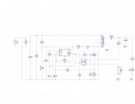
I had 15 mins on my own PC to look at the schematic you have and make some adjustments
1) You should add an input line filter eventually, although it can change the transfer function of the converter so needs to be properly designed. Worry about that later.
2) Class Y cap from primary to secondary ground. Not strictly necessary but leave a place for it on the board in case you need to add it later
3) Layout. Keep high current loops small and use thick traces. This includes the U1/C3/Q1/R8 loops, they should all be close together. Minimise the trace inductance in this loop by keeping traces short and fat.
4) Schottky diode clamps on the OUT pin of U1 as close as possible to the pin to protect it from voltage transients which comes from the gate charging and discharging. They should be included in the tight gate drive high current loop.
5) Your oscillator (R6/C4) appears to be wired wrong in the circuit. I've corrected this as per the datasheet.
6) The voltage adjustment pot R14 should be wired as a variable resistor and the feedback voltage to the TL431 taken from above this. This is mostly because any resistance of the pot in series with R12 will change the AC characteristics, but changes in the resistance between this node and ground aren't really important for AC (if the resistance is too low, the GBWP pole of the TL431 will shift down and that could still cause problems. This is because R12 and R14 in parallel set the gain of the TL431). Another reason for this configuration is so that if/when the wiper of the pot momentarily disconnects from the track, you won't have an open loop oscillating to potential damage, but rather the voltage will drop to the minimum as if R14 was a fixed resistor. Remember also that the output voltage has a significant influence on the AC characteristics of the loop. When designing the TL431 circuit you have to design for a specific output voltage and there is only so much you will be able to turn that pot to fine tune the output without potentially causing instability.
7) I've added the local compensation capacitor to the TL431 that provides the zero for type II compensation that current mode control tends to need. This will give the TL431 high DC gain and therefore tight DC regulation. I've also added a bias resistor bypassing the optocoupler LED which is generally a good idea as the TL431 is like an opamp which gets its power through its output pin.
8) I've also added a capacitor in parallel with R5. This capacitor is in parallel with the optocoupler's parasitic capacitance which together set the type II compensation pole. The parasitic capacitor in the opto is generally dominant and highly variable between devices and in a single device at different currents and temperatures and changes as the device ages. This generally sets the limit of crossover frequency and bandwidth for the entire loop. Optos suck. You don't strictly need this capacitor as the parasitic capacitor is the more important one, but it's good to put it there to give some form of control over this pole.
9) I've put a 20 ohm resistor in series with R11 and R12 (this is sometimes 50 ohm). This is for loop response testing and could be replaced with a a zero ohm link or jumper when not testing the loop, but it doesn't really affect anything by being there as its much smaller than R11 and R12. Good practice to put it in even if you're not going to test the loop any time soon. Testing the loop (and testing the opto AC response) is necessary to ensure stability especially as optos define the stability and are quite unpredictable (did I mention optos suck). Traditionally you'd need to rent some seriously expensive equipment to test the loop, but I've been working on ways to avoid the use of this.
10) I've rearranged the UC3843's error amp configuration so that you can bias it off and directly inject the feedback into the comp pin. I haven't used this IC before but from the datasheet description it looks like it should be possible because it's an open collector opamp. Just pull the Vfb pin low with a resistor and the output transistor will be in cutoff and this takes the onboard error amp is out of the equation. I think the polarity is right, as the TL431 is the inverting error amp and the emitter follower configuration of the opto should be non-inverting. The way it is in yours looks like you have it set up with a high gain, low bandwidth inverting amplifier and I can't see how that'd work [the gain would be -R4/(Zout of the opto), 150k divided by a few ohms, therefore loosely set high gain positive feedback]. This is the part I'm least sure of as I don't have the part in my hand and I'm doing this in my head.
11) I've added 2 possible snubbers in green. You'll likely need these to avoid the kind of oscillation you've seen, I'll let you research how to calculate their values. Getting a waveform of the Q1 drain voltage DC coupled on the scope would be useful.
You will likely also want to measure the magnetising and leakage inductances of the transformer on an LCR meter and output capacitor's ESR (It should be a low ESR type. The ESR zero frequency is important to know when designing the compensation for the loop and in current mode control output voltage ripple is proportional to ESR up to a point).
More reading for you:
http://www.eetimes.com/design/power...7/Power-Tip-17-Snubbing-the-Flyback-Converter
http://www.onsemi.com/pub_link/Collateral/TND381-D.PDF
http://switchingpowermagazine.com/downloads/15 Designing with the TL431.pdf
Best of luck!
Matt

 offline.jpg9.5 KB · Views: 160


