Hello guys,
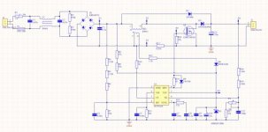
I built a CCM PFC circuit using a NCP1654 IC from On Semi to get 390 V that I feed to an unregulated DC/DC-Converter that powers a Class D amplifier. It is supposed to operate in wide mains from 85 V up to 265 V and have a maximal output power of 300 W.
The DC/DC-Converter works with 100 kHz +-20kHz so I choose the switching frequency of the PFC to be 200 kHz so I won't get differential tones in the audio spectrum, as the other frequencies of the chip are 65 kHz and 133 kHz.
Additionally my choke becomes smaller.
My circuit is able to operate and provides a stable output off 390 V when I power the IC with an external supply. As component count and size is a matter, I would like it to operate from a bias supply using an auxiliary winding from the choke. But then my output voltage is not stable enough and the PFC is not able to operate in wide mains.
I've come to the conclusion, that this is connected to my other problem:
In audio applictions the power needed to drive the speaker is very low. With all the other devices in my audio amplifier I will need about 10 W in idle mode.
As far as all datasheets and other literature, CCM ICs are not able to work properly below 20 % of their rated output power. That is also the power level at which the IC transits between CCM and CrM/BCM.
With 300 W rated output power, 20% means 60 W, which is way above what I need, so at 10 W the IC is working in CrM/BCM or in the case of the NCP1654 it goes into burst mode. In this burst mode the supply voltage through the auxiliary winding to the IC is not stable enough, so that it is average 9.5 V. That means the IC shuts itself down to protect itself and so the output voltage is not well regulated and therefore the auxiliary voltage is also not stable. That is the reason why TI suggest powering up the IC with an external supply instead of my bias supply method.
When I draw 64 W from the Class D amplifer at the end of my supply chain at 4 R (measured at the load) at high line (230 V), the PFC transits to CCM and I get a very stable PFC output voltage with almost no ripple voltage.
At 180 V I am able to get into CCM at just 32 W.
All the literature I read suggests, that I might have choosen the wrong topology for my project. But when I look at the datasheets and eval boards from TI, ST, Fairchild and On Semi and other topologies like CrM/BCM, FCCrM, interleaved and bridgeless designs, I come to the conclusion, that they will also fail when the power drawn is very low compared to the rated maximum output power.
Does anybody have some suggestions on how to proceed further? A new design? Another topology? A low power supply for idle mode and a high power PFC?
In addition, my PFC disturbs the mains heavily or radiates, as I can hear the pulses on the radio in the next room.
Thank you for your help and advices.
PS: The primary reason for the PFC is the ability to draw the same power from the line either in 100 V or 230 V mains. Only a voltage doubler for 115 V to 230 V would mean less output power, when the device is connected to 100 V mains.
Attachments
-
 PFC CCM NCP1654.jpg20.5 KB · Views: 155
