Problem in Sepic converter

falcosms

New member
Hello all

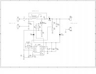
I made a sepic converter with UC3843. But i had problems with the regulation and current behavior in the mosfet.

the input is 10 ~25V and output is 14V 0,8A.

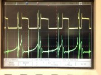
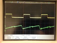
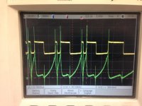
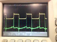
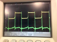
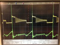
When the input is above 14V, the current in mosfet is good, but under 14V, the current is not correct, like the attached waveforms, output current of 500mA.

I have tried to change the frequency and inductor values (240uH, 500uH, 1,2 mH) but i don´t have sucess.

Anybody can help me?FORM-ABOVE-14V (Copy).JPGsepic-problem.jpgFORM-UNDER-14V (Copy).JPG
 

Jagd.Panther

New member
Please post pics of the PCB (top & bottom).

47R Rg looks way too much for a mosfet with 150nC Qg. Decrease it to 5-10R, you may try to shunt it with a diode to speed turn off.


Check if the oscillator is stable (probe Ct with a scope). Check if PWM power supply is way too noisy.
 

falcosms

New member
Hi there

thanks for the answer.

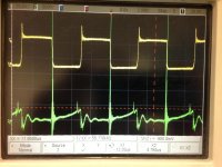
I have tried with Rg with 10R and 22R, with 47R, when the input is above 14V, the wave form is good, like the last picture.

I put a diode in parallel to Rg, but it doesn´t resolve the problem.

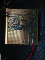
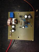
the IC supply and oscillator are ok, the pcb board is a prototype, please see the photos:

placa-inf.JPGplaca-sup.JPG
 

Jagd.Panther

New member
Are you 100% sure the oscillator is stable in bad case? UC3843 can't generate more than one pulse per clock by design, but that's what we see on the attached waveform. Can you please probe OSC & gate at the same time to see if that's the case?
 

Jagd.Panther

New member
The board looks sub-optimal, most of the traces are much longer than could be (didn't check for any errors though). Try to search for appnotes for integrated DC/DC converters (like MC34166/167 to get an idea how the layout should look like).
 

falcosms

New member
hi there

i noted that exists a noise in the oscillator when the mosfet waveform becames wrong. With a 10R gate resistor, the waveform became worst. With a 68R resistor, the problem surges with inputs of 11~8 Vcc.

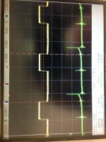
i noted a problem: in the next pictures, exists a peak current after the pulse of uc3843 goes to zero. I think is related with the LC group..

one picture is the gate and osc wave and another the current and gate driver.
gatexosc.JPGgatexcurrent (Copy).JPG
 

Jagd.Panther

New member
Can you test this converter with 100-150v mosfet? Like IRF540z, IRF3710z. (or probe voltage at mosfet's drain, it shouldn't exceed 40-50v for 55v mosfet).

Try adding a diode (preferably a 100v schottky one) from drain (cathode) to ground (anode).
 

KX36

New member
I won't say anything for definite about it as I can only really do buck derived converters in my head, but I can give some vague thoughts

- C30 looks out of place for that IC. You may want to remove it and rethink your compensation. Don't neglect the RHP zero (in continuous current mode)
- You have no slope compensation. You probably need it as duty cycle increases.
- You probably want to put a resisitor (around 1k) between C35 and R6 to make an RC filter for noise immunity/leading edge blanking on the current sense line. To actually reduce the noise you may need to improve the layout. (The PC I'm on can barely open the forum, let alone the photos, so I haven't seen them.) This resistor also can be a place to add slope compensation.
- D10 could be replaced with a schottky for higher efficiency and faster recovery time and therefore potentially less noise (in continuous current mode).
- R6 seems a bit low value for the current you're talking about, but I haven't calculated it. You might find that when the noise on Isns is reduced it can come up.


Edit:
Jagd.Panther, did you notice that the suspicious waveform is at 5us/div whereas the rest are at 2us/Div? That might be a clue as to how it appears to be pulsing more than once per cycle, but I don't have an answer at this point.
 
Last edited:

2hartanto

New member
Try to clean all soldering flux with paint thinner. After that add a sheet of cooper or brass to bottom layer and connect as much as possible to that new ground plane. Also add more capacitor from VCC to ground. If you have tantalum will be better. Add zener too from VCC to ground to clamp VCC at 12V ( if you do this don't forget to add resistor to limit current from D11 and D12)
 
Last edited:

2hartanto

New member
That sheet should hover above all soldering pad. Maybe 1.5mm to 2mm. Then cut the sheet edges you want to connect to ground, bend it and solder it to ground.
 
Last edited:

falcosms

New member
Hello all

thanks for the answers.

you are right, i forgot to put the current sense resistor in the pin 3. In my board it exists, but not in schematic.

my board is a prototype, not a final layout.

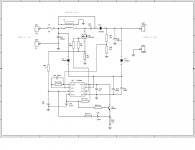
i removed the C30 and i search in the web about slope compensation, here is my new schematic:

sepic-2-page-001.jpg

now the circuit is more stable. In my calculations, the inductor had a inductance of 240uH and I peak of 1,74A - according with AN of Ti: http://www.ti.com/lit/an/snva168e/snva168e.pdf

for the current sense in uc3845 - 1V / 1,74 A = 0,57R, i put 2 x 1R parallel resistor. but with it, the waveform is this:

SEPIC1 (7) (Copy).JPG

with a r sense of 0,1R i had this waveforms:

SEPIC1 (1) (Copy).JPG

SEPIC1 (3) (Copy).JPG

Perhaps my inductor are not good? i put two separated inductors instead of the coupled, but the effect are the same.

sincerely


C30 looks out of place for that IC. You may want to remove it and rethink your compensation. Don't neglect the RHP zero (in continuous current mode)
- You have no slope compensation. You probably need it as duty cycle increases.
- You probably want to put a resisitor (around 1k) between C35 and R6 to make an RC filter for noise immunity/leading edge blanking on the current sense line. To actually reduce the noise you may need to improve the layout. (The PC I'm on can barely open the forum, let alone the photos, so I haven't seen them.) This resistor also can be a place to add slope compensation.
- D10 could be replaced with a schottky for higher efficiency and faster recovery time and therefore potentially less noise (in continuous current mode).
- R6 seems a bit low value for the current you're talking about, but I haven't calculated it. You might find that when the noise on Isns is reduced it can come up.
 

falcosms

New member
hi all

in continuation of my saga, i checke that i made a mistake in calculation of inductor.

the correct value is 100uH (checked in software calculator of Wurth electronics). but the problem persists.

i made a inductor with core EE25 with 10 turns of wire and i manually have changed the gap, in a moment, the smps works stable in all input range, but the ipeak is a little high (4,5A). i measured the inductance of L and i found 6uH...

check the waveform:

IMG_1201 (Copy).JPG

I don´t understand why with an inductor with low inductance run correctly..
 

KX36

New member
The low value inductor circuit is likely running in discontinuous current mode. That makes it intrinsically more stable than CCM and also there is no RHP zero in DCM; but the peak currents will be much higher than CCM and all your switches, inductors and series capacitor have to take those higher curent peaks. Still, I would have thought you could do it DCM considering the low power. SEPIC's something I don't personally have a lot of experience with.
 
Last edited:
Top