First smps

Silvio

Well-known member
Well, I just figured out why it failed.... Stupid me wired the High output from the IR2110 to the low side mosfet and the Low output to the high side mosfet on the PCB... Arghh!! Do you suppose I could just fix it with a jumper while I am still testing until I make the final PCB? I'm thinking both mosfets may be burned up at this point but perhaps the IR2110 survived? I'll have to check it out later.

Hi Brady, usually when the fets blow they go short on all pins. The driver attached to them is also blown and don't chance it or at least make a simple oscillator with another 3525 or IR2153 and check it out on the bread board with 12v and low current setting. feed 2 LEDs instead of fets and check waveform with scope. check also your driver chip as what is usually connected to fets will get the full 320v across, check also diodes and resistors. BTW do you have a spring powered solder pump? I usually use wick in delicate places only.
Yes you can cut the traces and re-route with insulated wire (keep them short as possible) If it works satisfactorily you can leave them there why the hustle making another pcb? Oh now I remember you are to make it regulated in the future and have to add components.

Take a look here for the start up see what this guy did
http://320volt.com/en/2x60-volt-smps-devresi-sg3525-etd44-ir2110/

regards,

Silvio
 

brady

Member
I removed the mosfets and IR2110 and indeed all were fried. I also found that the fuse blew as well. While they were out i did a load test on the startup supply and found that it brought it up to 10 volts with a 80mA ohm load attached. The resistor was just barely warm and the transistors weren't warm at all. I did the load test for about one to two seconds, and i believe it could safely work for a bit longer before getting too hot. I also checked the startup waveform and it rises up nice and sharply. So, I think the startup supply is pretty solid. I have also tested the supply connected to a SG3525 oscillator circuit and it began oscillating successfully. I'm going to go ahead and fix the board and put in my spare IR2110 and mosfets. If these blow I'll have to wait for more to come in.

Regards,
Brady
 

brady

Member
I fixed the swapped traces and installed new mosfets and confirmed that they are switching before doing a live test. When I did the test the first thing that happened was the LM7812 burned (im guessing I over volted it). So apparently I have too many turns? So now I have an external low voltage supply connected in place of the regulator temporarily. When I turned it on it made this awful switching noise. I kept it on long enough to measure the voltage waveform outputting from the auxilliary and its only peaking at 5 volts. When I measured across the primary I measured almost no voltage. I'm not sure what to make of it honestly.

I apologize if it seems like I am working haphazardly. I just don't really have any experience with these.

Regards,
Brady
 

Silvio

Well-known member
HI Brady I guess your half wave is only with one diode. I would first try and fit the second diode for rectification of aux supply and see what it puts out. you can also try to light a small 12v lamp 5watts or so to see what power is coming out of it. 5v no load is no big deal. What is the expected voltage according to number of turns of the aux supply? where you testing out with the full input voltage at the bulk caps?

regards

Silvio
 

brady

Member
There must be something fundamentally wrong with my driver setup, which seems to be causing a lot of the other problems. I ended up with the IR2110 turning into a dead short across the AUX supply again and I believe it took the high side fet with it as well (I see 132 ohms across any of the three pins). The low side fet seems to have survived. I believe this is what killed the regulator previously mentioned.

I am using a 10uF electrolytic capacitor and MBR1100 rectifier for the high side float supply on the IR2110.

My aux supply has 7 turns so peak voltage should be 170*(7/25) = 47.6 volts. I can't do full rectification unless I rewind the transformer for a center tap or add a bridge. I think I'll have to go back down on the turns or add a series resistor like you mentioned. Currently I don't have an easy way of adding the series resistor but it is possible. I also did check the bulk caps and they were reaching full voltage. However I can't fix that until I solve the driver issue.

Any thoughts?

Regards,
Brady
 

MicrosiM

Administrator
Staff member
@Brady

I am not sure if I understand you correctly, those 47V are supplying the IR2110?

In reality, the IR2110 driver can be your shortest way to success if you know how to deal with it, and can be your worst driver choice if you don't understand how it works.

I suggest that you read some IR2110 Application notes.

Hope that helps
 

Silvio

Well-known member
Hi Brady what I learnt here is that your low voltage supply has to be stable and regulated and well decoupled otherwise disturbance may occur to your circuitry. Why don't you try an external supply feeding the low voltage end. Hook up a small 8VA 14 volt trafo with a bridge rectifier and a smoothing cap followed by a 7812 regulator I guess this will sort things out.You can also try a wall wart. One other thing you should buy a 100w lamp and put it in series while you are testing it saves components it really works. A normal resistor does not work like a lamp. A lamp is low impedance with a cold filament and high when hot. The change in state is rather quick,

Hope that helps

Silvio
 

brady

Member
@Microsim

47 volts is the theoretical peak of the pulse from the auxilliary winding. Since there is no inductor or resistor in series with the diode I believe the bulk caps will match that voltage? If so I will need to either add series resistance or lower windings. Either way, this voltage is fed through a 12 volt linear regulator before being used by the driver IC.

@Silvio

I have a 12v 200mA transformer on hand that I could use for just that purpose. I may also be able to find a wall wart to make things easier. I have a feeling noise on the auxilliary supply line might be the culprit as you said. I need to get my auxilliary supply under control so that it doesn't burn out the regulator and hopefully then it will be okay.

I just discovered the hard way that the transistors in my startup circuit cannot tolerate very much reverse voltage (emitter to base) because both were fried along with the 11 volt zener. I'll be adding a diode in series with the emitter in hopes of fixing that issue. With the extra voltage drop I may want to bump up the zener to 12v. (note that I am using two transistors in a darlington configuration so there will be effectively 2 base-emitter drops and a diode drop).

The driver IC also has a bypass ceramic capacitor directly adjacent to the IC.

To avoid burning up more components I'll take your word on the 100W bulb.

Now that I thought of it, there was a lot of ringing on the output of the auxilliary winding. Maybe that is what killed the regulator?
Regards,
Brady
 

blasphemy000

New member
The maximum input voltage for an LM7812 is 35VDC. This is true for the LM78xx from 5V to 18V models, the 24V model's maximum input is 40VDC. I wouldn't recommend using these types of regulators with the maximum input voltage as the larger the drop across the regulator, the more heat has to be dissipated in the regulator for the same amount of current drawn through it.
 

brady

Member
Hello,

I got more parts in and did some testing. Probing revealed significant crossover on the two input lines and ground bounce at the mosfets. It looks like I'll have to do a redesign of the board. This time I will use ground traces to separate the input lines as much as possible and ground the input separately from the output, while keeping the output grounds as close as possible to the source pins. I skimped on several capacitors on the first design so I will be sure to include those in the second iteration (10uF aluminum and 470nF ceramic on high side and low side drive supplies). Hopefully with these changes the driver will be more robust and I can avoid killing more chips with the transients it was experiencing.

Along with these changes, I will be adding the corrections I made to the startup supply, adding a resistor to the output of the auxilliary winding, and adding the option for more capacitance at the output of the voltage regulator.

Regards,
Brady Riddle
 

Silvio

Well-known member
Hi Brady,

Its good to see that you managed to find what was causing the fets to blow. Transients are no good at all and I learnt that signal to fets must be clean as possible. In my case I decoupled the chips as much as possible on the supply input to them. In fact each chip has its own decoupling caps in my case 22uF and 100nf close to each chip and also at the input of the traces carrying the aux supply. In my case I have a separate small switching supply which supplies the pwm fed from the main bulk caps. I found this on an air conditioner pcb and pressed it into service. It can deliver around 500ma at 15volts. I chose this option for compactness as it occupies less space on the board than a normal trafo caps regulator etc. It happened that it had a half a second delay on the low volt output which will allow the bulk caps to charge before the output emerges from it. Regarding the output capacitance I have 1000uf which I think is more than enough followed by a small 1mH choke and more decoupling (22uf & 100nf) near the entrance to the pwm board. You can take a look at my PDF 1000w smps and see what I mean.
I grounded mine on two points one near the bulk caps and the other near the source of the low side fet .Magnetic field exists everywhere near the smps and careful planing will pay back in the end result.

One last thing I'd like to mention is that you need a steady smooth supply powering your pwm and fets and see that finally you have it otherwise you will be in for more hustle.

Anyways etching a new board with modifications will surly bring out better results. Until then I await your progress and results.

Good luck

Regards,

Silvio
 
Last edited:

brady

Member
Hello,

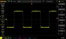
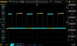
I rebuilt the circuit and fortunately the gate drive appears to be working perfectly. I currently am running the circuit from a separate auxilliary supply so it is currently not self-powered. I was able to make some measurements.

1) The rectified output of the auxilliary supply at full duty cycle is 46 volts DC, so I will definitely have to reduce the number of turns to prevent burning up my regulator.
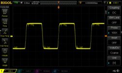
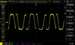
2) The primary waveform is pretty good at full duty cycle, but becomes unrecognizable when lowered any.

Please look at the waveforms captured below, and keep note that I did testing with no output stage or load. (secondary windings floating)

Main_Output_Full_Duty.jpg
MosfetGates.jpg
Primary_Full_Duty.jpg
Primary_Low_Duty.jpg

Regards,
Brady
 

brady

Member
Update:

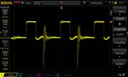
I finished assembling the output stages and did more tests. Turns out that it only has problems at very low duty cycles. When you get near the minimum duty cycle, the gates of the MOSFETs show spikes and the transformer becomes very noisy.

I still do not have a load attached. Do you have any suggestions for what I could use as a load?

Regards,
Brady
 

Silvio

Well-known member
Hi Brady, I am not so experienced in this field of work but I like to share my taught with you. It seems to me that especially in the last capture I can see that the rise time becomes slow and hence the slope. The rounded edge on top of the wave form could be that somehow the switch off is not sharp and it seems that the fet is going in linear mode in this period. (try lowering gate resistors) I guess some charge is left until it switches off. Check also the supply voltage entering your PWM in this period just to make sure it still holds the voltage. One other thing that is coming across my mind is that the bootstrap capacitor may be too large and its not discharging quickly enough hence the slow turn off.

I have an idea that might eliminate any issues coming from inductive kickback from the trafo is placing a normal 40 watt bulb instead of the transformer primary. This will approximately draw 20 watts due to it being rated at 240v and only having half the voltage across it. This way you can check again the wave form and see what happens.
As for your auxiliary indeed 46v is way too much. Before you dismantle the trafo for this winding see if you can fit the right amount turns (these should be 3 or 4 turns more or less) on top of everything on the trafo just to experiment what is best. I am just remembering that it would be better to have a fixed auxiliary supply this will not tend to have low voltage issues on minimum duty cycle. In ATX this supply is independent from the rest of the circuitry.

good luck

regards Silvio
 

brady

Member
okay, I haven't removed the transformer yet but I did measure the gate of the high side. It goes without saying that it looks horrendous (see picture). So something is causing the high side gate to act funny.

DS1Z_QuickPrint1.jpg

Regards,
Brady
 

Silvio

Well-known member
I am not sure if you are using the same pcb or you have made another one.
try some ferrite beads on the jumpers to the gates
you can try beads directly on the fets gate lead

I can see ringing when the fet switches off. Could that be some form of coupling from another source for example when the other fet is switching on.
What I see here is that its the period where the other fet is switching on and coupling somehow and ringing is produced. This ringing is being produced after the dead time from what I can see.
Try a small ceramic cap across the gate and source 10-20pf see what happens. Just trying to decouple the gate but if you can find the source where it is coming from it will be better.

regards

Silvio
 
Last edited:

blasphemy000

New member
How are you probing the high side gate? Improper probing of a floating high side switch can cause all sorts of issues. A high-voltage differential probe is the proper way to do it, but they are expensive and most people don't have access to one.
Also, the IR2110, when used with a boot-strapped high side supply, doesn't work very well at very low duty cycles. The capacitors that store the charge to drive the high side gate get charged up only while the low side switch is turned on. If the low side switch has a very low on-time then the bootstrap caps may not fully charge and can cause the high side to switch erratically since it does not have enough charge to drive it properly. This might not be your issue, but it's something to check for.

Brad
 

Silvio

Well-known member
Blasphemy000 Just a small question to you. In your opinion what will be the best way to switch the gates in a regulated supply? Is it with a gating trafo? Or there is another way while still using the IR2110?

Regards,

Silvio.
 

Silvio

Well-known member
@ Brady, I have been reading on the IR2110 on Tahmid Blog and reading further on through the posts it was said by Tahmid that the IR2110 can be driven from 0-100% duty cycle only if you have an isolated supply driving the high side gate. It is for sure that when he said this it was through experience and in your case it may be the cause you are having funny waves on low duty cycles. here is the link and read the posts on February 20 2013, link http://tahmidmc.blogspot.com.mt/2012/10/magic-of-knowledge.html

Lower your gate to source resistors to 1k. You can try lowering also your gate resistors to 4,7 ohms instead of 10. I have seen circuits with IR2110 driving 1RF460 fets in this configuration.


Regards Silvio
 
Last edited:

brady

Member
I am not sure if you are using the same pcb or you have made another one.
try some ferrite beads on the jumpers to the gates
you can try beads directly on the fets gate lead

I can see ringing when the fet switches off. Could that be some form of coupling from another source for example when the other fet is switching on.
What I see here is that its the period where the other fet is switching on and coupling somehow and ringing is produced. This ringing is being produced after the dead time from what I can see.
Try a small ceramic cap across the gate and source 10-20pf see what happens. Just trying to decouple the gate but if you can find the source where it is coming from it will be better.

regards

Silvio

I am using a new PCB design. I made a jumper to shorten the lead connecting the source pin of the high side and that didn't change anything. I also made the gate resistances larger and that didn't change anything. Thing is, it seems to work perfectly at maximum duty cycle. I can also lower the duty cycle some before things go wrong. As others said, maybe I just cannot lower it that much with the bootstrap supply. However, even though I can lower the duty cycle some, it doesn't effect the output voltage. I'm thinking this could be because I don't have a large enough load, is this correct?

Regards,
Brady
 
Top