OK wally7856, I'm back with my results.
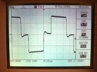
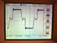
These are 14 pictures of oscillograms obtained while I made changes over the last corrected version of the schematic.
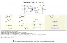
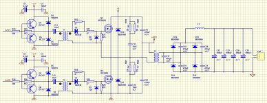
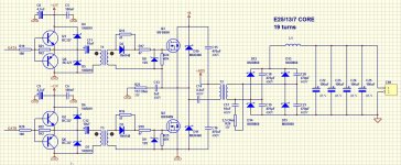
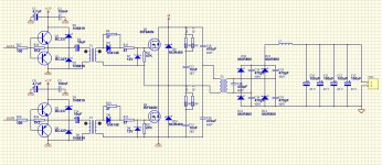
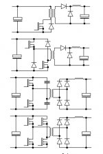
The new version of the schematic is also attached in this post.
Starting with this last circuit, I first added a 4.4uF polyester capacitor as you suggested. The capacitor should had been 4.94 uF, but I tried to make it fast with the components I had in stock.
Then I worked on the transformer secondary adding resistance to the existing 470pF as you suggested.
In the middle of the tests I found secondary results, and made some other removals and changes.
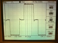
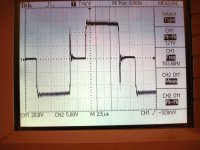
Because of my error, I made the tests with 2A load instead of 4A. I am sorry for that and for sure I will have to rework all the values with the correct load. I don't have all the component values but I will get them for wednesday.
So these tests have been done by combining values in series and parallel to get best approximations.
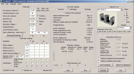
To follow the changes I suggest to look at the previous version of the schematic so we can follow parts numbering.
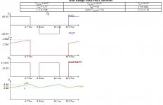
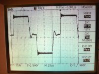
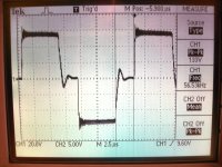
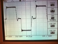
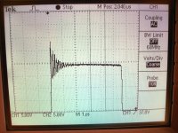
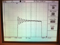
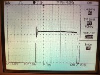
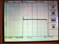
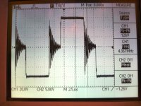
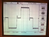
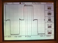
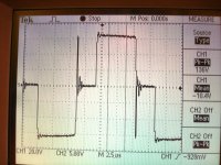
All oscillograms measured across transformer primary terminals
Oscillogram 1: added 4.4uF polyester capacitor in series with transformer primary
Oscillogram 2: tested 5.9uF value instead of 4.4uF
Oscillogram 3: tested 2.2uF value instead of 4.4uF , I finally left 4.4uF
Oscillogram 4: added 1K resistor to C17 - 470pF ceramic disc capacitor, this capacitor has very slight effect on the top ringing of the waveform
Oscillogram 5: completely removed C17 - 470pF ceramic disc capacitor, this capacitor has very slight effect on the top ringing of the waveform
Oscillogram 6: ringing detail C17 removed
Oscillogram 7: replaced C17 470 pF by 10nF, has great impact controlling ringing
Oscillogram 8: testing 2.5 Ohm in series with 10nF C17, top ringing very much reduced, I take this values as finalOscillogram 9: Completely removed MOSFET's snubbers R19, R20, R21, R22, C15 and C16 - brutal ringing
Please switch to last corrected version of the schematic ( attached )
Oscillogram 10: installed just one snubber network C13 10nF + R23 112 Ohms
Oscillogram 11 and 12: adjusted value of C13 now 5nF + R23 112 Ohms
Oscillogram 13 and 14: increased load from 2A to 4A, new glitch !
This is the result of my tests, I think I have to rework all values with 4A load.
Now we can talk some issues if you agree.
Kind regards
 SCHEMATIC.jpg732.9 KB · Views: 65
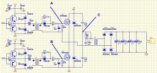
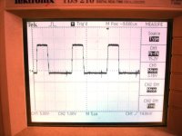 SIGNAL A.jpg214.9 KB · Views: 34
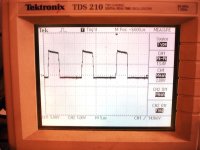 SIGNAL B.jpg210.9 KB · Views: 25
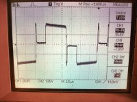 SINGNAL C.jpg242.2 KB · Views: 36
")