regulated TL494 based SMPS

res_smps

Member
Dear all,

is there anyone interested in SMPS using TL494?
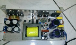
i am developing a SMPS using TL494 (because cheap and easy to find here), but i don't have enough time improving it
- it is regulated, TL494 placed on primary side, with GDT to drive mosfet (because i found so many counterfeit IR2110 here so i choose GDT)
- isolation using optocoupler, not GDT
- no additional auxiliary supply for TL494
- EPC4649S core for main transformer

this is my progress so far :
regulated +-45V, (using TL431 as error amplifier, not just a zenner)
down to 44,9V in 200W load
down to 43,6V in 380W load

i will attach schematic and picture, and simulation files later

terima kasih,
res
 

res_smps

Member
why I cannot edit or delete my previous post?
for schematic in post #2
without no load output voltage is Vzener+2v
with load connected output is Vzener

for GDT I use toroid core for EMI filter, with 2mH primary inductance (21 turn)
GDT winding 1:1:1
 

Attachments

  • core emi.jpg
    core emi.jpg
    76.1 KB · Views: 115
  • gdt.jpg
    gdt.jpg
    58.8 KB · Views: 135
  • proto.jpg
    proto.jpg
    344.6 KB · Views: 231
Last edited:

KX36

New member
You can only edit a post up to 30 minutes after posting it.

The schematic looks mostly reasonable. A couple of things I would have done differently. A few notes:

Normally I'd say not to use the TL494, but I understand where you're coming from.

R42 voids your isolation. You'll have to remove that, I assume it's there for prototyping only, it shouldn't be doing much anyway. Also in terms of isolation I hope you wound the transformer with properly rated tape and margins, that your PCB has a sufficient creepage distance between primary and secondary and that capacitor C35 is class Y.

Have you stabilised this? I don't see any proper compensation on the schematic to do so. I noted the simulation you put in another thread was oscillating and I think I gave some tips there about it. You're only regulating the positive rail and the negative is only regulated by the linked inductor. That's fine though, just be aware the regulation on the negative rail won't be quite as good.

The coupling capacitor C14 for the GDT primary is probably not necessary. Don't use it if you don't have to, it introduces a potential resonance between itself and the magnetising inductance of the GDT primary which has to be damped which increases the impedance of the driver which slows switching. R14 is similarly of questionable necessity. Try with and without on your prototype.

The C18/R31 snubber. Snubbers tend to only really work when both R and C are close to the ideal value. I hope you've calculated or prototyped to get the right value and not just copy and paste it from another design. RC snubbers burn quite a lot of power (P=f.C.V^2) It's presumably there to damp the resonance between Q1 or Q2's parasitic capacitance and the transformer's leakage inductance, although I'm not sure it's in the right place to do so, it should be in parallel with the capacitance. Please feel free to explain it to me. I might just be having a daft moment.

Regards,
Matt
 

borysgo2

New member
KX36

Could You explain me one thing please. I am going to do some regulated smps based on sg2525, and I do not know wihich way to choose for fedback.
Plan A
Secondary --> zener network + resistor + optocoupler
SG2525 side--> error amp used + compensation

Plan B
Secondary --> type II or III compensator based on LT431
SG2525 --> pulling COMP pin no 9 to GND with optocoupler.


Thanks for any information.


res_smps

I see You are not using the internal errror amps of tl494, tell me please how pulling COMP pin is doing the job at the dynamic loads ? Have you made any tests ? I am curious because I am prototyping my first regulated smps and have huge lack of knowledge.

Regards
 

res_smps

Member
res_smps

I see You are not using the internal errror amps of tl494, tell me please how pulling COMP pin is doing the job at the dynamic loads ? Have you made any tests ? I am curious because I am prototyping my first regulated smps and have huge lack of knowledge.

Regards


hi borysgo2,
I never got success using error amplifier and optocoupler (Tl494 on primary side), audible noise came out from transformer.
many commercial smps i have seen always put tl494 on secondary side without optocoupler

yes, i have made prototype (post#4)

then I found this link http://www.trifolium.de/netzteil/kap8.html
and adopt it to my circuit

please check my simulationView attachment TL494sim.zip
 

borysgo2

New member
Thanks !!
I have made a driver board prototype with SG very similar like from link above and it seem to work OK by pulling COMP pin to regulate PWM.
For now I will have to finish up universal smps prototype from rubbish parts.

Regards

s2.jpg
s1.jpg
 

borysgo2

New member
OK
So I have done some tests and maybe it can be usefull (or maybe not).
I have made feedback circuit with tl431 type III compensator + pulling COMP pin in controller.
After I have tweaked the components values the regulated half of the supply is superb.

If I will apply/remove load approx 8A @ 112V the output voltage ripple does not go over 200mV (there is no overshoot and output is regulated really quick to stock value with 5mV precision), I can put the square wave load and the ripple will not be higher than 200mV. It is really OK.
But if I will apply the load at the non regulated half of the secondary --> the voltage ripple is very high at that half.

That is why I have stopped to develop regulated version for of SMPS.
IMHO the best and easiest solution would be to putt PFC in front of smps to minimise the mains ripple and voltage drop.

Regards
Peter
 

res_smps

Member
OK
So I have done some tests and maybe it can be usefull (or maybe not).
I have made feedback circuit with tl431 type III compensator + pulling COMP pin in controller.
After I have tweaked the components values the regulated half of the supply is superb.

If I will apply/remove load approx 8A @ 112V the output voltage ripple does not go over 200mV (there is no overshoot and output is regulated really quick to stock value with 5mV precision), I can put the square wave load and the ripple will not be higher than 200mV. It is really OK.
But if I will apply the load at the non regulated half of the secondary --> the voltage ripple is very high at that half.

That is why I have stopped to develop regulated version for of SMPS.
IMHO the best and easiest solution would be to putt PFC in front of smps to minimise the mains ripple and voltage drop.

Regards
Peter

Hi peter,
I also stopped developing regulated smps for dual output

did you use separated or coupled inductor?
i have experiment with coupled inductor, when i put high load on one output, output voltage became unbalance
 

borysgo2

New member
Yes I was using coupled inductor, I even got special cores with ''flexi'' inductance, at light loads they have higher inductance and it is decreasing with load.
The well made not regulated one is working really OK, just need a few more caps at the primary side.

Regards Peter
 

MicrosiM

Administrator
Staff member
I agree with using a PFC at the SMPS front, that the best option to maintain the sound qualiy and solve the related problems to ripple, etc...
 
Top