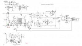
The TL494 it looks like you're using while at first glance seems OK for half bridge as it's voltage mode control, the part itself is obsolete and not recommended for new designs. It's a general purpose PWM IC rather than a SMPS IC and so it does things strange ways.
IIRC, the compensation of the on board error amplifier doesn't work as expected. It's kind of backwards, so if you look at your typical type III opamp compensation with the voltage divider from output to IN- with RC across the top resistor and RC from the FB pin to IN- and a reference voltage on the IN+ formed by a voltage divider down from the internal 5V reference. In the TL494 however, you have to have the reference to the IN- pin and Vout to the IN+ pin, which means the compnesation is on the reference side of it rather than the Vout side. So, the series RC from Vout to IN+ should be from Vref to IN-.
I wouldn't expect to see the electrolytic capacitor on the FB pin, don't know what it's doing, can't imagine it help stability.
Typically with a pot to adjust the output voltage, you'd want it out of the AC feedback loop so that it doesn't affect stability, which means making it the lower resistor of a voltage divider. You also would typically want to set it up so that the input voltage to the error amplifier doesn't go up and down but rather stays in the linear region. The error amplifiers in SMPS chips are very primative opamps and won't behave well near their rails. You have 2 pots to set the voltage. I can't see really how one is a set point and one is a set limit like they're labelled. If it's a regulated power supply you should only need one pot and possibly a resistor or 2 in series with it to set its minimum/maximum position.
The TL494 has 2 error amps OR'd together, and it's very tempting to set one up for voltage limiting and one for current limiting, but this will behave very poorly. the IC has no internal latching, so current limting will result in many switching transitions within a single switching period. i.e. high frequency oscillation dramatically increasing switching loss. Also, the half bridge topology is unsuitable for current mode control which is essentially what you're trying to implement by doing this. The bus voltage between the capacitor divider will be pulled to one of its rails by positive feedback and the transformer will saturate. Doesn't really matter if you're regulating the primary current or the output inductor current in this regard, although there is inherently less protection when you have no current limiting on the primary.
For a half bridge, the minimum IC I'd recommend is a SG3525 or equivalent (I like UC2525A). It can be interfaced directly with a gate drive transformer or hi/lo gate driver IC, has a more textbook design and incorperates features such as latching, UVLO, totem pole outputs, soft start etc, all of which are really required of a proper SMPS.
")