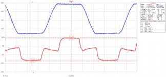
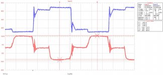
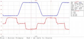
what should the loaded primary waveforms on a 1KW SMPS look like?

Mschuckel

New member
Hello All! I am a long time follower and first time poster. I want to thank everyone here for the vast wealth of information that you have made available!!!

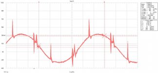
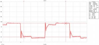
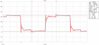
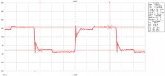
I have designed a new 1KW SMPS based on the SG3525. This SMPS is designed using sufrace mount components where possible. This SMPS is running well with no load. But when I place a 700W load on the unit I see this waveform:
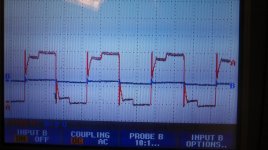
2013-09-12 10.50.49.jpg

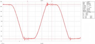
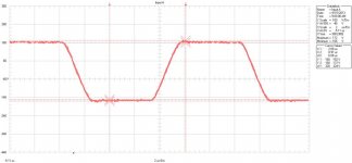
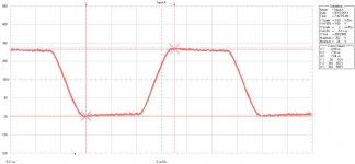
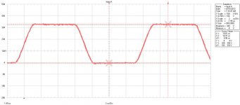
When the SMPS is running with no load I see this waveform:
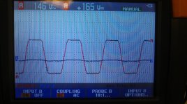
2013-09-12 10.38.02.jpg

My question is this:

dose the loaded waveform look even close to normal or do I have work ahead of me?

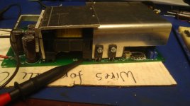
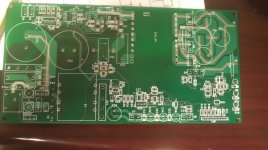
I have attached some more pics of the SMPS below:
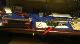
2013-09-12 10.38.18.jpg2013-09-12 10.38.29.jpg2013-09-12 10.38.52.jpg

Thanks and keep up the great work!!
 

MicrosiM

Administrator
Staff member
The design looks neat and clean. Good Work :UP:

I am not sure if that wave is taken from the primary side of the transformer?

Please show waves across the below

DS of each Mosfet while SMPS is loaded, and while SMPS is not loaded.

What is the temperature of the MOSFETS heat sink when loading the SMPS 700W? and for how long?

Dont forget that the heatsink you show is SMALL for such power!!

What is the running frequency of this SMPS?

Show me wave across the series capacitor with the primary of the transformer. while SMPS is loaded.

that looks like a regulated SMPS? for audio?


Regards
 

Mschuckel

New member
Sorry about the delay. I was out of the lab this weekend. I attached a bunch of wave forms taken as you requested.

I have run 700W load tests on the supply for up to 5 minute durations and the MOSFETs are around 140 degrees F after 5 minutes. The output rectifiers are 150 Degrees F in the same time frame. This board is slated to be a battery charger once I get the thermal issues put to bed.
Thanks again for all you help.

Mschuckel


Across_SeriesCap_700W_LOAD.jpgAcross_Seriescap_NO_LOAD.jpgPrimary&SeriesCap_700W_LOAD.jpgPrimary&SeriesCap_NO_LOAD.jpgQ1_DtoS_700w_LOAD.jpgQ1_DtoS_NO_LOAD.jpgQ2_DtoS_700W_LOAD.jpgQ2_DtoS_NO_LOAD.jpg
SSC1_C.jpg
 
Last edited:

MicrosiM

Administrator
Staff member
Spkies?

This seems to be a regulation problem, I am not sure.

The schematic you are showing is too small, please upload it as PDF file if you can.

Also regulated SMPS without proper inductor at the output will put more stress at the switching devices.

I recommend that you change these Mosfets with something like 12N60A4D IGBTs

You must put a capacitor in series with the primary of the GDT

The most strange thing into your waves is the spikes, I think you have to disconnect the regulation loop and TRY without it it first, to confirm if the regulation loop is responsible for these issues. Because most waves seems to be fine without the spikes.

Reaching 140C after 5 minutes of operation for Mosfets will never make this supply succeed.

One important thing, in IDLE without LOAD, does the Mosfets heat sink heats? and how many C after how many Minutes

My SMPS used to heat up to 85C after 5 Minutes 1200W Loaded.

Regards
 

Mschuckel

New member
This seems to be a regulation problem, I am not sure.

The schematic you are showing is too small, please upload it as PDF file if you can.

Also regulated SMPS without proper inductor at the output will put more stress at the switching devices.

I recommend that you change these Mosfets with something like 12N60A4D IGBTs

You must put a capacitor in series with the primary of the GDT

The most strange thing into your waves is the spikes, I think you have to disconnect the regulation loop and TRY without it it first, to confirm if the regulation loop is responsible for these issues. Because most waves seems to be fine without the spikes.

Reaching 140C after 5 minutes of operation for Mosfets will never make this supply succeed.

One important thing, in IDLE without LOAD, does the Mosfets heat sink heats? and how many C after how many Minutes

My SMPS used to heat up to 85C after 5 Minutes 1200W Loaded.

Regards

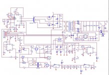
Sorry about the schematic:) Can't upload a PDF but I improved the resolution this time.

I will try the IGBTs you recommended. I will also include a series cap on the GDT.

Currently the regulation loop is disabled.

The SMPS idles with no thermal issues at all in fact I ran it for several hours early on with no sign of MOSFET heating.

View attachment 4340

Thanks for the ideas!

By the way have you seen these parts By 'ROHM' SCT2080KE the specs look great!

Mschuckel
 
Last edited:

Mschuckel

New member
Thank you!! I will look into this in detail. This GDT was off the shelf and It is a 1:1:1 ratio with 3 mH windings. I will attempt find a transformer with much lower inductance. (say the 300uH range)

I will post the results!!
 

Mschuckel

New member
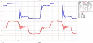
Still waiting on parts right now. I have looked at the GtoS wave forms on both MOSFETs. I believe I see distortion in the drive waveforms that would account for the primary waveform distortion under load. I believe that Q2's drive is getting corrupted. Now I must figure out where the distortion is corrupting the drive circuit and how to remove it. I will keep you all updated as I proceed. Again thank you all for you help and comments!!!


Q1_700w_load_primary w_respect to gate.jpgQ1_no_load_primary w_respect to gate.jpgQ2_700w_load_primary w_respect to gate.jpgQ2_no_load_primary w_respect to gate.jpg


Mschuckel
 

Mschuckel

New member
OK, I have changed the MOSFETSs, Rewound the transformer (using info from the latest transformer calculation program), and I enhanced the driver circuit using 2 totem pole drivers (to increase gate drive current). None of the changes yeld any improvements in output power??

Still researching this. Suggestions are welcome

Mschuckel
 

Mschuckel

New member
I am still fight the same problem I posted pictures of earlier.

I have severe output waveform distortion that radically increases as I attempt to increase the load (to the point of hearing the SMPS Hiss). I have traced this problem to the SG3525 IC?? I have verified that the SG3525 output PWM is radically changing when heavy loads are placed on the SMPS. (Loads that should be within its capability)

I will send you more wave forms later today. I have now got proof that the SG3525 is the culprit. I am carefully looking at all of the pins around the SG3525 in hopes of seeing the culprit pin. i.e. voltage changing, reference distortion etc.

I am now looking at using a PIC microcontroller to generate the drive wave forms. I know that the PIC will be immune to these types of problems and will allow me to load the SMPS without the noise messing up the output.

More Soon:)

Mschuckel
 

Mschuckel

New member
Ok, I have rewound the transformer using calculations from the "SMPS Transformer calculation tool 4.0". The new transformer is doing very well at nearly 900W loads. Still see the Xformer start to thermally start to run away after about 5 minutes or so. I am working to remedy this with the next transformer. I also figured out what was causing the waveform distortion under heavy loads. I appears to be inductively coupled signals from the transformer that are causing oscillations in the SG3525 circuit. I made a few location changes in the driver circuit and resolved this issue completely. I am now looking at laying out the PCB again keeping this issue as well as others in mind with the hopes that the next revision will be better behaved.

I will keep everyone posted.

Mschuckel
 

KX36

New member
I know I'm chiming in a little too late but..

Note on temperatures; he said 140'F, which is 60'C.

Is this meant to be a quasi-resonant or hard switching converter?

I don't have a lot of experience with HB, and really we need a legible schematic to work from, but the first waveform posted looks like the "1/2 Vin" voltage in the input capacitor divider (or just that across the series cap) is changing significantly through the cycle, which doesn't seem right if it's hard switching, nor do the gentle slopes under no load really.

Use of SG3525 would suggest hard switching... I see no output inductor, but I do see an RC snubber across the transistors, which obviously would change the waveforms to a degree and it does make me wonder if this is meant to be quasi resonant and whether you've designed the inductance into the transformer and the "snubber capacitor" is the resonant cap... I assume not, I'm just thinking out loud to myself here... Really need a clear schematic. I can't even comment on the feedback loop design..
 

Mschuckel

New member
I will post a schematic later today. The feedback circuit is a small high speed voltage to PWM converter. it monitors the DC output voltage and converts it into PWM. The PWM is then passed through a high speed optocoupler and converted back into an analog 0-5V signal that will be used by a future Micro controller. I also have continued research on the transformer and discovered that I may need to shield it to help prevent the feedback issues I have been fighting.

Thanks for your reply!
 

KX36

New member
I don't really know what to make of this. It's certainly unorthodox. If I were to integrate a microcontroller into an SMPS, I'd make a traditional SMPS with the usual analogue control loops and use digipots/DACs and transistor switches to interface the microcontroller to that. With regard to your secondary side LTC6992 voltage-set PWM chip. You'd be better off using an actual PWM IC designed for use in a feedback loop, with a built in error amplifier such as.. say.. the SG3525 you already have used. It's perfectly possible to have the regulator on the secondary side controlling switches on the primary if that's what you want. The PWM IC would need an aux power supply and there may be issues of race conditions between the 2 power supplies etc and if you drive the gate drive transformer from the secondary to the primary it will need to have the same full isolation specs as the switching transformer, something most GDTs don't need. I've designed a secondary side PWM before in an offline power supply to ease integration with a (secondary side) microcontroller.
 
Top