You are using an out of date browser. It may not display this or other websites correctly.
You should upgrade or use an alternative browser.
You should upgrade or use an alternative browser.
Gate Drive Transformer Issues
- Thread starter twenglish1
- Start date
sanumar001
New member
sanumar001
New member
does not have a oscilloscope. The fact is that the transistor punches.
sanumar001
New member
little way out and check with ociloskopu is not as long as no one sg3525 pwm and neviksta. when I start to increase the pwm and then punches.
sanumar001,
First thing I notice is there's no resistor between gate and source of the IGBTs. I'd put 10k on each of them to stop them from spuriously turning on.
To troubleshoot your problem, get an oscilloscope and look at the IGBT gate waveforms. You need to know if they're turning on and off completely and quickly. If this is powered from the mains you need an isolation transformer but from your input voltage it looks like it isn't.
sanumar001
New member
Thanks for the reply. Power Schemes only 50V-90v.dc I will try to follow your advice.
sanumar001
New member
Happy holidays everyone.
The trick is to start with a scheme GDT transformer. appears to have been an error of the scheme itself. Correction and works well.
maybe you can offer battery charging protection scheme? In order to set the limit load voltage battery charging disconnected automatically. The voltage has fallen to activate charging. Charger here will be used for wind farms. 48v charging system. Thank you.
Hello.
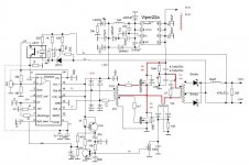
I do the battery charger according to this scheme. I asked for help, because initial start scheme extremely hot transistors. maybe what's wrong in the scheme. Transistors IRFP450 ThanksView attachment 5004
I just noticed that there is an error in gdt phasing..I mean the dots at gdt secondary are not correctly connected to the gates.
Yeah I frequently check the output of the sg3525 it hasn't changed since I posted the picture of the scope image, could my power supply not be supplying enough current?, roughly how much current should a toroidal GDT like I am building require?
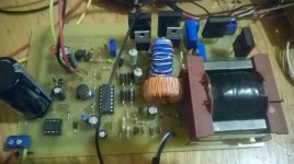
I thought I found a good combination of components for GDT circuit driven directly via 20 ohms connected from the output of SG3525 and to the primary of GDT because its secondary waveform looks fine..Is this pics and video a good indication of nice GDT waveshape?..pls comment..
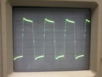
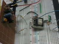
I omitted the video because it is upside down..
Last edited:
blasphemy000
New member
The down-sloping peaks of your drive waveform shouldn't be an issue just so long as the end of the slope is still holding your FET on hard. You don't want that slope to drop so much as to bring your FET back into the linear region of operation as this can cause massive heating in the FETs. If you want flatter tops to your drive waveform, you need to increase the primary inductance slightly by increasing the number of turns on your primary. To keep the output voltage of the GDT the same you would also have to increase the secondary turns to match. It shouldn't take much to flatten them out, maybe only a couple more turns. Also, I don't know what time-scale you are showing in your scope image, so I can't really comment on the rise/fall times of your wave. I try to keep my rise/fall times as fast as possible, but anything over ~200ns is just unacceptable for me. Overall though, it doesn't look bad.
Hi Blasphemy000,
I really appreciated your explanation about how good or bad my GDT waveform is..I will follow your advise in making additional turns in primary as well as in secondary because that is my idea too and thanks for the confirmation..I will post again the results as soon as I do it for your further comments.. Before, I thought there was no way I can make the wave to be flat until I got the idea of increasing the number of turns and now you confirmed it..I forgot to include the frequency,the time-scale you mentioned..That wave is running on 70Khz..and the peak before it slope down is 13v and down to 10v before it fall down..Its pulse time is 14 microseconds..I will try to measure also the rise/falll time of it to know if it still under your acceptable limit (not more than 200ns)..
Thanks and regards,
Demykiko
Hi Blas,
This is now the waveshapes pics after increasing the turns..there is improvement but only if the resistors are to be change also..but if the value of resistor is retained
the down-sloping peaks becomes worser than before..so I changed the resistor value for the gate (Rg) and also the resistor between primary and SG3525 to come up with that waveshapes as shown in the pics..the frequency is 60khz..1st pic time division is 2us..2nd pic time division is 5us..The problem is the rise and fall time which is .4 microsecond or 400ns if I correctly measured it.. What can you say?
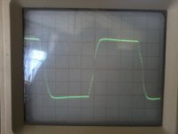
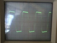
Regards,
Demykiko
This is now the waveshapes pics after increasing the turns..there is improvement but only if the resistors are to be change also..but if the value of resistor is retained
the down-sloping peaks becomes worser than before..so I changed the resistor value for the gate (Rg) and also the resistor between primary and SG3525 to come up with that waveshapes as shown in the pics..the frequency is 60khz..1st pic time division is 2us..2nd pic time division is 5us..The problem is the rise and fall time which is .4 microsecond or 400ns if I correctly measured it.. What can you say?


Regards,
Demykiko
Last edited:
blasphemy000
New member
I had a nice reply written out for this but my phone deleted it all. I will reply written I get back to my computer at home. I have a couple of suggestions for you.you. Just hang tightfriend.iend
It seems that my GDT waveform (previous posts) above works ok..Take a look at this video showing How good waveshapes provided by a GDT can make a good smps..Pls see the actions that take place because I added a little control over it by making it adjustable plus short circuit protection or overload..
http://youtu.be/klH8RxmuS_w
I'm sorry the video is not in proper position
http://youtu.be/klH8RxmuS_w
I'm sorry the video is not in proper position
Last edited:
blasphemy000
New member
I'm glad to see that you got it working properly. That's great. The <200ns rise/fall times aren't super critical(in some cases), it's just the goal I like to have in my power supplies to minimize heating in the switching devices. My power supplies are usually low-voltage(10 to 100VDC) but high-current(10 to 100Amps and I'm working on perfecting my design and increasing the current). I also like to push things to the failure point to ensure that my supplies will be reliable when operated under normal conditions. The faster my switching times are, the less heat is generated in my switching devices, and therefore my supplies can then withstand a longer duty-cycle before the switches overheat. I would imagine in a lower-power supply that having super-fast switching times would be less important just so long as there is no shoot-through and they are fast enough that the switches don't spend a ton of time in their linear regions.
Now, having said that. I reread some of your older posts and realized that you said you were driving your GDT directly from the outputs of the SG chip. Now, according to the datasheet these outputs can source/sink a maximum of 500mA but their recommended operating range is around 200mA. I also just noticed that the "typical" rise-time of the outputs is 100ns but can be up to 600ns. The "typical" fall-time is 50ns but can go all the way up to 300ns. Since you're driving the GDT directly from the SG chip, your GDT cannot provide a drive current to the FETs that is greater than the drive current going into the primary side of the GDT. Actually due to some transformer losses, the FET drive will be slightly less than the primary drive current. Too little drive current to the primary side of your GDT can also cause the slower rise-times and sloping tops. What happens is, when you increase the inductance of the GDT to minimize the sloping tops, the rise/fall times will suffer due to the greater inductance. If you have a way of buffering the outputs of the SG chip to provide a greater drive current(ie: Transistor Totem Pole) to the primary of the GDT you can then balance your rise/fall times and the voltage droop at the peaks by adjusting the inductance of the GDT. If you don't have enough drive current going into the GDT, achieving flat tops on your waveform will require way more inductance than is really necessary and your rise/fall times will suffer significantly. As you increase the drive current for the GDT, you can lessen the inductance of the GDT, improving the switching times, while still maintaining minimal voltage drop at the peaks.
Now, having said that. I reread some of your older posts and realized that you said you were driving your GDT directly from the outputs of the SG chip. Now, according to the datasheet these outputs can source/sink a maximum of 500mA but their recommended operating range is around 200mA. I also just noticed that the "typical" rise-time of the outputs is 100ns but can be up to 600ns. The "typical" fall-time is 50ns but can go all the way up to 300ns. Since you're driving the GDT directly from the SG chip, your GDT cannot provide a drive current to the FETs that is greater than the drive current going into the primary side of the GDT. Actually due to some transformer losses, the FET drive will be slightly less than the primary drive current. Too little drive current to the primary side of your GDT can also cause the slower rise-times and sloping tops. What happens is, when you increase the inductance of the GDT to minimize the sloping tops, the rise/fall times will suffer due to the greater inductance. If you have a way of buffering the outputs of the SG chip to provide a greater drive current(ie: Transistor Totem Pole) to the primary of the GDT you can then balance your rise/fall times and the voltage droop at the peaks by adjusting the inductance of the GDT. If you don't have enough drive current going into the GDT, achieving flat tops on your waveform will require way more inductance than is really necessary and your rise/fall times will suffer significantly. As you increase the drive current for the GDT, you can lessen the inductance of the GDT, improving the switching times, while still maintaining minimal voltage drop at the peaks.
I'm glad also that you had a time to explain your good point about the <200ns rise/fall times. I'm aware that making rise/fall times as short as possible is as much best attribute as making the peak of pulse flat to really lessen or possibly eliminate (exaggerated) the heat of switching devices.And that is my goal too for the SMPS that I'm currently working with.I'm also like you who want to push thing to its limit to know and ensure its reliability under normal operating conditions..And I already implemented it by trying to test the performance of SG3525 as it is directly driving the primary of GDT with only 5 ohms in between them, without considering yet the buffer as additional current driver for the GDT and also just to make parts count minimal.It is just to know what shape of waveform this can bring out and if SG3525 will become hot while operated in long time..But so far It seems the setup is working fine despite the rise/fall times are more than our goal with only little over shoot after the rise time..The PWM is not dissipating so much heat..The switching devices are not as hot as I expected. In fact I tried to extract 330 watts from a small toroid with 26.5 volts and 2 ohms load and surprised by the outcome that the two Mosfets stay cool..I don't want to imply here that using Transistor Totem Pole is not a good idea to consider..I admit that one of these days I will resort to using the buffer driver if the setup I mentioned before will not be really reliable over time..I'm very thankful to you pal because you are there to confirm my idea and all I have to do next is to follow them as expert's (you)advice.
twenglish1
New member
I have been away from this project for a while and just decided to check back on my thread, thanks for all the replys, lots of great info! i will be trying some of the suggested ideas within a few days or so, my issue had been, as seen in my original post, the output waveforms from the gate drive transformers are garbage, i will be using transistor totem-pole drivers, and will continue to experiment with building a good gate drive transformer, i have salvaged some EE ferrites from some PC powersupplies and an old TV powersupply, with bobbins intact! will post updates of my experiments

