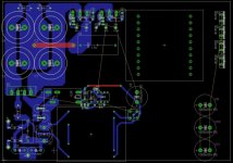
SMPS LAYOUT for best results
Hi luchni
If you really would like to make a new PCB layout, I advice you to inspire from the below layout
In order to get a robust results.
And in order to put the driver in front of the MOSFETS + making the SHORTEST signal path from IR2110 to the G of MOSFET. witch is necessary
Spend some time now, and you will make an excellent LAYOUT
Or you can proceed with that one.
Thank you
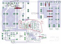
Attachments
-
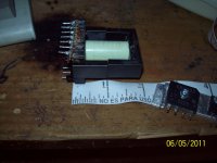
 DSC00925.jpg204 KB · Views: 1,581
") . Is it possible to add output voltage regulation to this circuit? That would be really nice for most users, so if i do another pcb design (i say maybe because i will be very busy in the next two months) i could squeeze that in there.
. Is it possible to add output voltage regulation to this circuit? That would be really nice for most users, so if i do another pcb design (i say maybe because i will be very busy in the next two months) i could squeeze that in there.